
Sleep-Awake Pulse Generator
The Avise Forth for selected ATmega CPUs includes a SLEEP command to reduce supply current drastically if no action is needed over a period of time. The internal ATmega peripherals only provide very short wakeup times. For this reason an external circuit was developed. It is an autonomous circuit that can be used for other tasks, too.
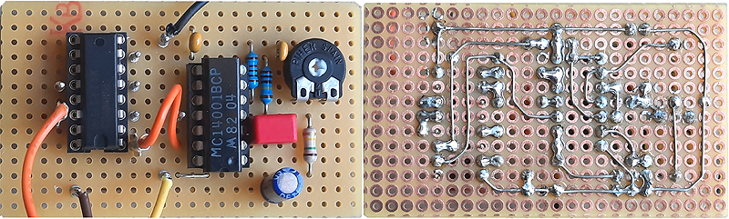
To make reconstruction as easy as possible, a single layer PCB with 2.54mm Veroboard compatible layout and standard through hole components is described here. Size of PCB is 63x38mm, including a 10mm fixing border.
Electronics details:
Essentially the circuit is built with a standard CMOS astabile multivibrator followed by a CD4040B asynchroneous counter.
With component values as shown in the schematic, the multivibrator pulse time can be adjusted in the range 0.4 to 3 seconds, with approx. 2 seconds when P1 is in center position. This is divided down by the CD4040B counter, pin connectors have been added each division/by4 position. So, together with P1 a continous wake-time up to approx. 90 minutes is provided. These parameters can easily changed over a wide range by simple user modification. Because ATmega PCINT interrupts react on every level change, the wake-time is 1/2 of the time, user simply would expect from the counter cascade (first low-to high after reset terminates SLEEP).
If the "Reset" input is pulsed to high level, it sets any output to low level (synchonize timing). Low "Reset" level keeps the counter active. If a special pulse shape is needed for awake, an optional inverter is on PCB. If not needed, it's input should be connected with a defined voltage level.
The prototype shown above is powered from a standard ATmega board, supply voltage in the range 3.0V (limited by CMOS parameters) and typically +5.0V (limited by ATmega parameters). The supply current depends strongly on the sum of R1 and P1: min.ca 7 Microamp (650 kOhm) and max. ca 28 Microamp (150 kOhm), essentially independent of value of C1.
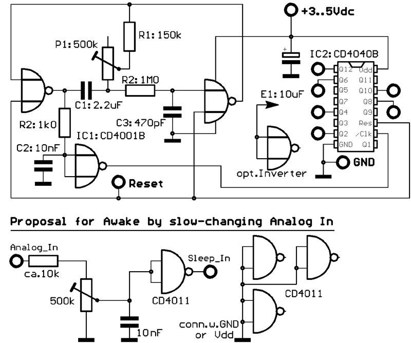
The lower part of the schematic shows a well-working circuit to keep the microcontroller sleeping until an analog input reaches a trigger value, set by potentiometer. The shown circuit triggers a falling pulse edge on rising analog input. If another inverter is hooked behind, a falling analog input is triggered. With two potentiometers and one IC, an awake trigger window is created. Instead of CD4011 NAND a CD4001 NOR can be used with the same result. These simple CMOS circuits use max, 2 Microamperes in the pulse transition area and perform a very sharp pulse transition (in contrast to High-Speed CMOS, which take up to 5mA and provide less straight pulses). The input resistor is only for overvoltage protection of the microcontroller, in most cases may be safely reduced to 1kOhm.
Download:
The subsequently downloadable material is copyrighted (c)2023 by Wolfgang Schemmert.
Assembly and use of the device is permitted for free by everybody for any purpose ("freeware")
All information is based on best knowledge, but without any warranty. Any responsibility is excluded.
Single layer Veroboard compatible PCB layout
(1:1 TIF format).
The layout is seen "through" the PCB from component side, as usually needed for PCB production.
* Right of technical modifications reserved. Provided 'as is' - without any warranty. Any responsibility is excluded.
* This description is for information only. No product specifications are assured in juridical sense.
* Trademarks and product names cited in this text are property of their respective owners.