
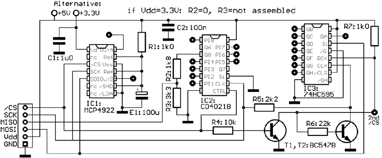
SPI based I/O expansion for CForth hardware
This module is primarily developed to provide more I/O for the STM32F042 based CForth hardware proposal. Because the hardware resources of this controller are quite rare and are strictly pre-organized on this PCB, the circuit design had to care for some restrictions. So only one /CS line is available for 3 different ICs.
Anyway, this circuit can be used by almost any SPI with 3.3V supply and 3.3V data level or with 5V supply and 5 or 3.3V data level. Specifically it is compatible with the STM32G431 hardware proposal and as expansion for the small CForth operated DMX controller.
To make reconstruction as easy as possible, a single layer PCB with 2.54mm Veroboard compatible layout with standard through hole components is described here. Size 70x47mm.
The circuit works as follows:
Idle state of the /CS line is "high". The D/A converter MCP4922 operates in its standard mode. The supply voltage is used as reference, filtered with a low pass 1kOhm/100uF. The input impedance of each reference input is ca. 165 kOhm, the input impedance of the /SHDN input is neglegible. So the reference is about 1% lower than the supply voltage. The MCP4922 needs a mode 0 (0,0) 16 bit SPI packet, the clock rate is uncritical in the range available here. Though the specification in the data sheet is unprecise, it has been tested here to work with 3.3V logic at 5V supply. The /LDAC input is grounded, so the input buffer is transferred to analog out at the rising edge of /CS. For compatibility with both other ICs, the 16 bit SPI is sent as a sequence of two 8bit SPI packets. As a side-effect, during this sequence the actual input of the CD4021 is responded automatically.
The CD4021 does not need any MOSI input. The parallel input levels are permanently latched to the shift register as long as /CS is "high". This is fixed as soon as /CS goes "low" and the last input level configuration is clocked out via MISO. For a processor with 3.3V logic, a voltage divider is necessary. To read the digital input explicitly, a single 8 bit SPI packet is exchanged. In this case, the MCP4922 does not change its analog output because it needs 16 SCK pulses while /CR = "low" to react. So, both devices are separated easily.
The 74HC595 has no built-in /CR selector and the byte received serially via MOSI is transferred to the parallel output with the rising edge at the RCK pin. Because connector CN4 of the referenced STM32F042 hardware provides only one pin for use as /CR (PB1), the inverted /CR (T1, R4 ,R7) is used for chip select. An 8bit SPI packet is transferred while /CR is "high", so it is ignored by the other ICs. Next a short "low" pulse is put on /CR, which causes the rising edge at the RCK pin. Additionally with T2, R5, R6 the SCK pulses for 74HC595 are suppressd while /CR is "low".
The actual CForth firmware for STM32F042 provides a set of SPI signals at CN4: SCK=PA5, MISO=PA6, MOSI=PA7. Additionally /CN=PB1, +5V and GROUND are available at CN4, so the additional SPI module can be attached with a single connector. The "PB1inv" pin of CN4 could be used instead of T1, R4, R7 (see pinhead "2nd /CR" near pin9 of IC3). But for general fitness this was not used at the described circuit.
For use with other SPI master, unfortunately no SPI devices else can be operated with this construction. In this case, a separate /CR line would be needed for the 74HC595 instead of T1, R4, R7 (use pinhead "2nd /CR"), but the SCK pulses must be suppressed with T2, R4, R6 while this second /CR is high.
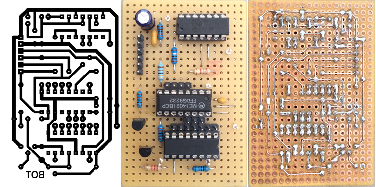
Veroboard compatible PCB design, size=70x47mm.
The layout is seen "through" the PCB from component side, as usually needed for PCB production.
CForth programming example for STM32F042:
//this way code is compatible with hex and decimal number base
//recommended LQFP32 wiring:
//SCK is PB3, MISO is PB4, MOSI is PB5
0xB7 varcon /CS; //Port PB7 works as /CS
//recommended TSSOP20 wiring:
//SCK is PA1, MISO is PA0, MOSI is PA4
//0xB1 varcon /CS; //Port PB1 works as /CS
//recommended Nucleo L576 wiring:
//SCK is PB3, MISO is PB4, MOSI is PB5
//0xB8 varcon /CS; //Port PB8 works as /CS
//once init SPI and /CS idle state:
/cs oh
0 8 0x18 ini-spi; //about 100kHz clock with STM32F042
: ispi 0 8 0x18 ini-spi ;
//limit DAC input 12bit
( DacValue -- DacValue )
: limit dup 0xfff > if drop 0xfff then ;
//0x3000 sets MCP4922 config bits for DAC A over input and split into 2x8bit SPI
//first SPI command returns CD4021 parallel input
( DacValue -- digIn )
: dacout 0x3000 or dup /CS ol -8 shift spi swap spi drop /CS oh ;
//send prepared output to DAC A, returns CD4021 parallel input
( DacValue -- digIn )
: dao limit dacout ;
//change config bit for DAC B
//send prepared output to DAC B, returns CD4021 parallel input
( DacValue -- digIn )
: dbo limit 0x8000 or dacout ;
//get parallel digital input from CD4021
( -- digIn )
: pi /CS ol 0 xnop 0 spi /CS oh ;
//send parallel digital output to 74HC595
( digOut -- )
: po /CS oh spi drop /CS ol 5 xnop /CS oh ;
//simplified command to send parallel Out and receive Parallel In
( digOut -- digIn)
: pxch /CS oh spi /CS ol 0 xnop spi /CS oh ;
: test do 0xf0 pxch .h 0x800 ms again ;
Download:
The subsequently downloadable material is copyrighted (c)2020-23 by Wolfgang Schemmert.
Assembly and use of the device is permitted for free by everybody for any purpose ("freeware")
All information is based on best knowledge, but without any warranty. Any responsibility is excluded.
Single layer Veroboard compatible PCB layout
(1:1 TIF format)
* Right of technical modifications reserved. Provided 'as is' - without any warranty. Any responsibility is excluded.
* This description is for information only. No product specifications are assured in juridical sense.
* Trademarks and product names cited in this text are property of their respective owners.